Panel and through-hole plating
Provide the panel dimensions, feature range and where deposit thickness is measured.

Specify a PCB copper-plating anode by the plating step, bath and waveform, panel geometry and deposit acceptance criteria.
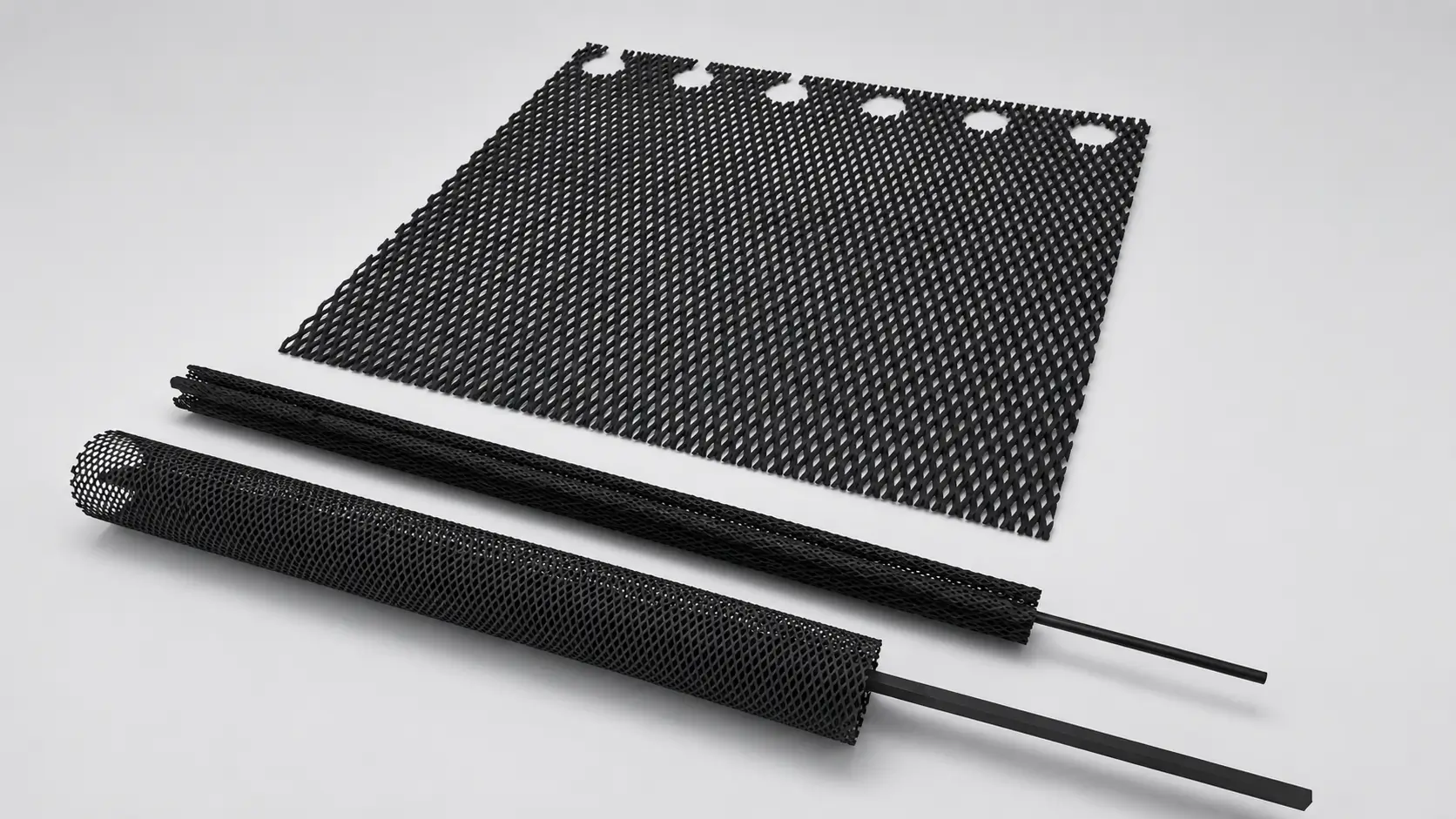
A replacement can fit the tank and still present a different active face to the panel. Compare the electrode and fixture with the required copper distribution across the panel and through its features.
Provide the panel dimensions, feature range and where deposit thickness is measured.
Identify the station and quality targets. Share the rectifier waveform and bath supplier’s operating window where available.
Evaluate the anode against the controlled bath and electrical regime, then check the arrangement around the moving or stationary panel.
| What to compare | What to provide | What it helps confirm |
|---|---|---|
| Bath and additives | Send bath type, chemistry and additive package or vendor specification. | Which anode coating warrants testing with the approved bath. |
| Current waveform | Identify DC or pulse duty and supply the rectifier schedule and load range. | Whether the comparison covers the actual electrical duty. |
| Panel and anode position | Share panel width, anode spacing, shielding and fixture location. | Which active face, envelope and mounting arrangement can be evaluated. |
| Deposit acceptance | Provide the thickness map or via-fill acceptance criteria and current defect pattern. | How to judge a trial using the panel conditions that matter. |
Review mesh or plate electrodes as candidate formats when the line is designed for insoluble anodes. Confirm coating compatibility with the bath and establish how trial panels will be evaluated.
Compare cell, bath and fixture inputs for coated-anode inquiries.
Prepare the drawing, current waveform and qualification requirements.